Institute of Semiconductor Physics SB RAS
Novosibirsk, 630090, RUSSIA
*Lavrentyev Institute of Hydrodynamics SB RAS
Novosibirsk, 630090, RUSSIA
Representative solid amorphous dielectric layers are devoid of anisotropy, and in this sense, their properties are close to those of liquid dielectrics. At the same time, solid amorphous materials are more homogeneous than liquids, because they have no impurities such as vapor bubbles. Moreover, the high mechanical strength of solid phase as compared with liquids prevents developed flows of materials when local energy releases, and suppresses cavitation.
The microelectronic technology produces uniform films of 10--1000 nm thickness, and high electric fields ~ 106 -- 107 V/cm can be reached at 10--100 V applied, which is far less than the voltage ~ 100 kV used for the liquid breakdown.
These facts allow one to investigate the breakdown of solid amorphous films over a wide range of external conditions to analyze possible mechanisms of breakdown conformably to the dielectric liquids. Up to now, experimental data on breakdown in model systems such as solid amorphous films has not been used to analyze the results of research in the liquid dielectric breakdown. At the same time, an understanding of the stochastic regularities of the amorphous films breakdown is a step forward in testing the relevant theoretical models of liquid dielectric breakdown. And vice versa, statistical approaches that are well suited and applied widely in analyzing experimental data on breakdown of dielectric liquids can provide new information on the breakdown of solid amorphous films.
One important characteristic that indicates the physical mechanism of breakdown is the statistical time lag of its initiation.
Let us consider the initiation of breakdown in the uniform constant field between plane electrodes. We divide the electrode surface mentally into m small elements of the same area Ds = S / m . It is reasonable to suppose that:
P = (1-p)(i-1)m m (1-p)(m-1) p .
Within the limit of high and low values of m and t, respectively, we derive the probability distribution function of the statistical breakdown time lag:
f(t) dt = mS exp(-mSt) dt . (1)
Hence it follows that for plane electrodes, the mean value of the statistical time lag is < ts > = 1 / m(E) S . The known typical shape of the sharply descending dependence < ts > on the electric field strength is primarily due to this sharply increasing dependence of the function m(E) .
The breakdown electric strength Eb of insulators is commonly defined for a 50% breakdown probability given a fixed voltage pulse duration. The influence of electrode area on the electric strength is evident from the requirement of equal breakdown probabilities for the same time. For plane electrodes, m(Eb ) S = m(Eb0 ) S0 . In the short pulse range, the dependence Eb(S) is very weak because of the strong dependence m(E) . For example, for the fluctuation model of breakdown in dielectric liquids [1,2], m(E) = A exp(E / g) . In this case, we have
Eb = Eb0 + g ln(S0 / S) . (2)
Empirical data are generally approximated by a relation such as Eb = Eb0 (S0 / S)d . Alternatively, these experimental data are well described by function (2) and can be used to determine the value of g and, hence, m(E) . For example, for water, d » 0.1 [3], and it turns out that, for g = 0.082--0.083, these functions agree with an accuracy of 2% over a range of S/S0 from 1 to 100.
The form of the function m(E) is determined by the physical mechanism of initiating the breakdown. Given this function for a specific material, one can calculate all statistical regularities of its breakdown.
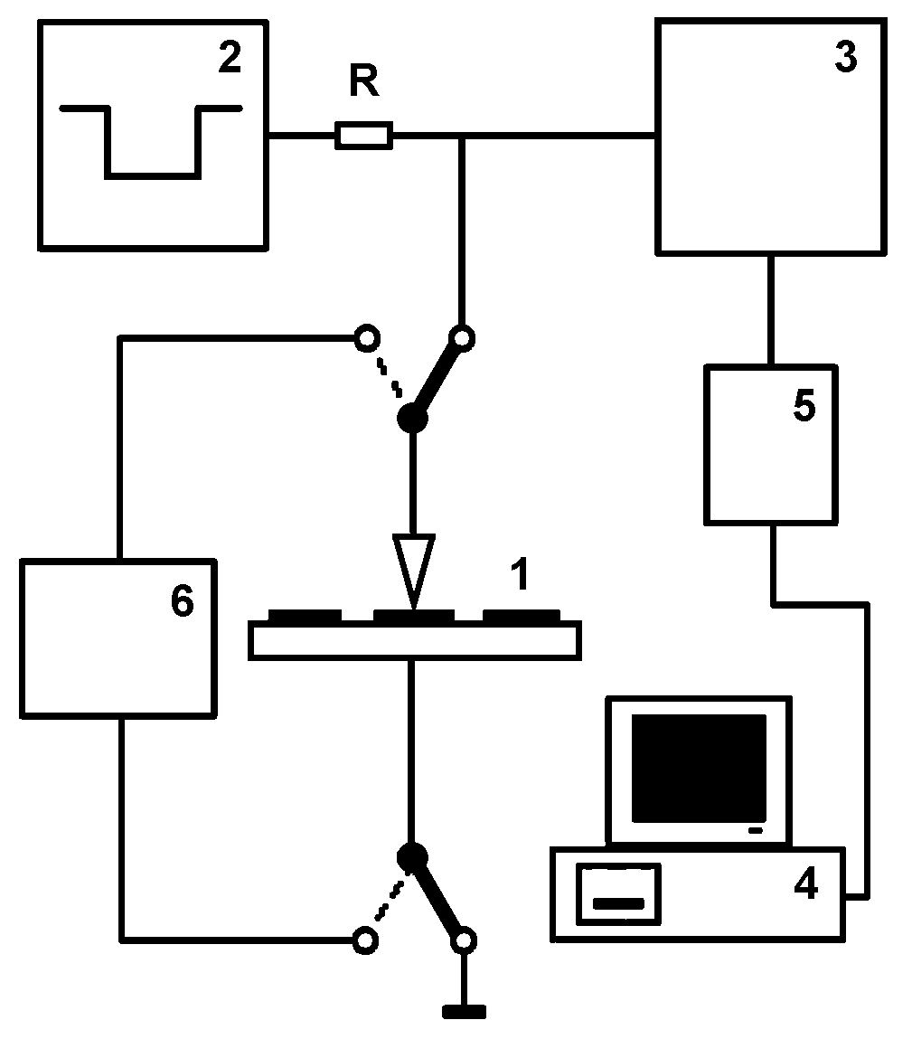
The samples consisted of a silicon substrate of the p--type conductivity and a thermal silicon dioxide layer of 102 nm thickness. The top side of the dielectric film was coated with a matrix of 0.7x0.7-mm aluminum electrodes. With these electrode dimensions, in the range of field strength amplification due to of the edge effect the breakdown probability was ~ 10-3 and could be neglected.
Stochastic properties of breakdown of the above films were investigated using an automated recording and computing system (Fig. 1).
Rectangular negative voltage pulses with amplitude V and a duration t0 = 10 ms were supplied to an aluminum electrode of the test MOS-structure (1) from the single-acting pulse generator (2). The rise time of the voltage pulse was about 0.1 ms and was mainly determined by the charging of the MOS capacity through the internal resistance of the generator (RC = 0.09 ms). Short microsecond intervals were measured by the digital time-interval meter (DTM) (3), which was connected to the computer (4) using the IEEE-488 interface card (5).
In the given scheme, the leading edge of the voltage pulse initiates the time count by DTM. At time t after the beginning of action of a strong electric field, the MOS-structure breakdown occurs. This is accompanied by a sharp decreases in the resistance of the MOS-structure and, hence, by the passage of a short current pulse due to the discharge of its capacity. The MOS-structure voltage therewith decreases jumpwise and stops the time count. Evidently, if the dielectric breakdown has not occurred over the generator pulse width t0, DTM fixes the value equal to t0. All the time intervals (t or t0) measured by DTM are stored in the computer memory for further statistical analysis.
Measurements on each sample were began with pulses of a low amplitude, 36 V (dielectric field intensity » 3.5·106 V/cm). After each ten pulses the voltage amplitude was increased by 2 V until a dielectric breakdown happened. Before voltage supply and after breakdown, the voltage-capacitance characteristics of the MOS-structure were measured by the device (6) to check its charge state. Then, a tungsten probe sharpened electrolytically was placed onto a new MOS-cell.
For a real breakdown in the n-th voltage step, the statistical time lag tn was measured.
Stochastic approaches developed in the models of breakdown in dielectric liquids can be applied to the experimental data obtained using the value of m(E) . In this case, the probability that dielectric breakdown of the sample have not been occurred by the time tn in the n-th step at a stepwise increasing voltage is proportional to
P(t)=exp(-m(En )Stn) $\prod \limits_{i=1}^{n-1} $ exp(-m(Ei )S Dt) =e-H , (3)
where H = $\sum \limits_{i=1}^{n-1}$ m(Ei )SDt + m(En )Stn . Here Ei is the electric field intensity at the i-th voltage step, Dt = k·t0 , k is the number of pulses of the same amplitude (in our case, k = 10). From Eq. (3) it follows that H has the physical meaning of a dimensionless analogue of the statistical time lag. For an arbitrarily varying voltage, H = $\int \limits_0^t $ m(E)S dt , and this expression can be named the field action integral.
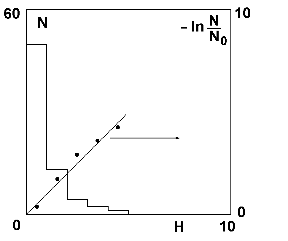
The number of samples Ni wherein no breakdown has happened to the i-th voltage step decreases with each step, Ni+1 = Ni - DNi , where DNi is the number of samples broken down at the i-th step. Upon integrating Eq. (1) from Dt to infinity we obtain the number of samples Ni+1 that remain intact after the i-th step: Ni+1 / Ni = exp(-m(Ei )S Dt) = exp(-DH(Ei )) . Hence it follows that m(Ei )S Dt = - ln(Ni+1 / Ni ) .
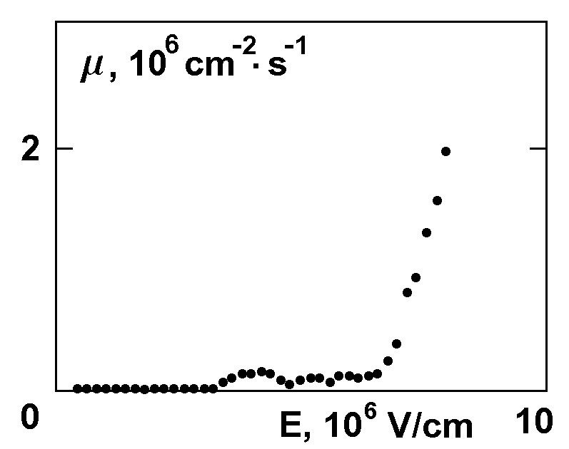
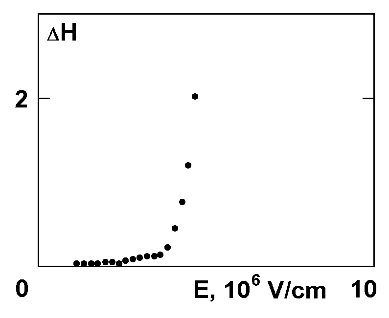
The dependence of m(E) obtained from the experimental data for the thin amorphous SiO2 layers is shown in Fig. 3.
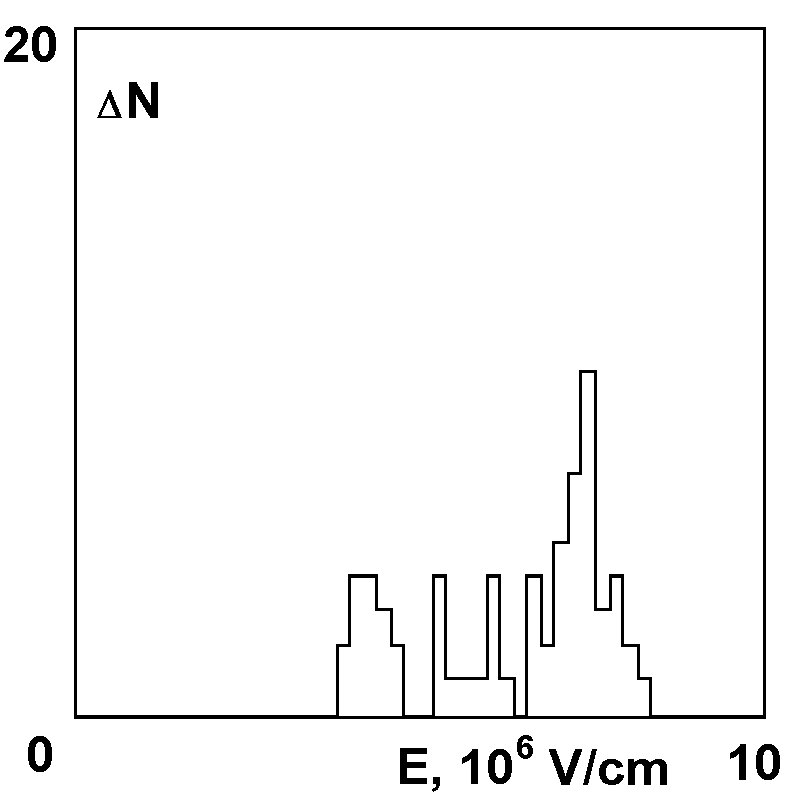
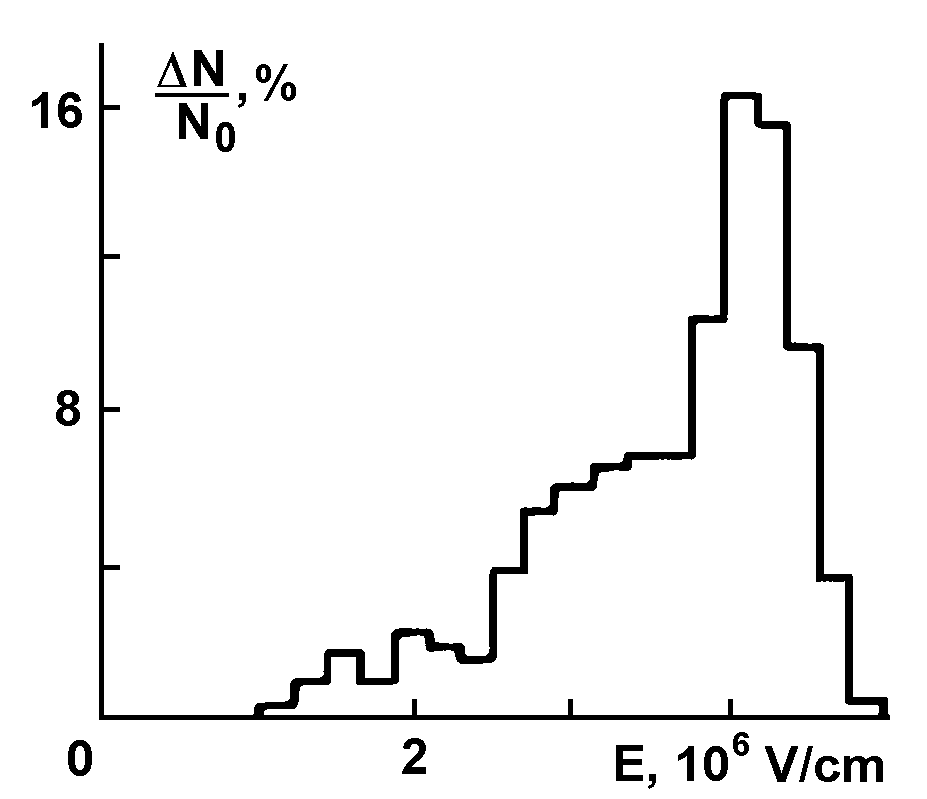
Using the experimental data for the breakdown of thin SiO2 layers and the above dependence of m(E) , we constructed a bar chart of the distribution of H values (Fig. 4) for which dielectric breakdown occurred. The shape of this dependence agrees well with the exponential distribution (3). The last is confirmed by the line behavior of -ln(N / N0) versus H . Here N0 is the total number of samples.
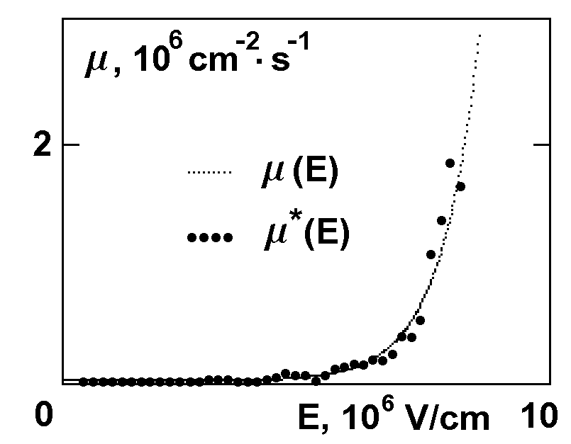
In a similar way as the above experiments, we performed a computer experiment in which a dielectric breakdown with rectangular, stepwise increasing voltage pulses was simulated. The fluctuation model of a breakdown involving a specified function m(E) = A exp(E / g) was used. An analogue of the experimental data was obtained for small statistical samples (N0 ~ 100). The dependence of the value of m*(E) restored by this set of "experimental" data agrees well with the original dependence (Fig. 5), and this confirms the correctness of the method used.
The method described herein was also applied to the experimental data of [5] on the breakdown of Lu2O3 layers (Fig. 6). Unfortunately, these experimental data were obtained in a quasi-uniform electrical field (a hemispherical upper contact electrode, d = 0.07 mm). In this case, the distribution function of the breakdown time lag has the form [4]
j(t) = $\int \limits_S $ m(E) ds · exp(- t $\int \limits_S $ m(E) ds ) ,
and the expression for DH takes the complicated form DH = DE / KE $\int \limits_S $ m(E) ds . Here KE is the rate of increase in field strength and DE » 2.2·105 V/cm is the electric field strength step in the the bar chart in Fig. 6. In this case, we were unable to obtain quantitative data on the function m(E) itself from the dependence of DH on the field strength (Fig. 7). The qualitative similarity of the dependences given in Figs. 3 and 7 suggest that correct interpretation of seemingly different bar charts (Figs. 2 and 6) can provide important physical information that has been missed in previous studies (e.g. [6]).
The results show that the breakdowns of thin amorphous solid films and liquid dielectrics have many features in common. Therefore, the information obtained in experiments with thin amorphous films is useful in simulating liquid dielectric breakdowns.